You're reading for free via Erik Engheim's Friend Link. Become a member to access the best of Medium.
Member-only story
Vector Processing on CPUs and GPUs Compared
SIMD, CUDA, SSE, MMX, SVE2 and RVV how different are these approaches to parallel processing?

Modern CPUs and GPUs can all process a lot of data in parallel so what exactly makes them different? This question is getting more relevant as you we see Arm processor add Scalable Vector Extensions, Intel and AMD adding AVX to the x86 microprocessor architecture, while RISC-V has recently formalized its RISC-V Vector extensions.
Apple is adding Neural Engines to their M1 System on a Chip (SoC) and we have recently seen Nvidia release their new Hopper H100 GPU architecture. Common to all these systems is that they aim to increase performance through the utilization of data parallelism. At their core these systems are SIMD systems, Single-Instruction-Multiple-Data. This contrasts with classic computer architecture which is Single-Instruction-Single-Data (SISD) as illustrated below.
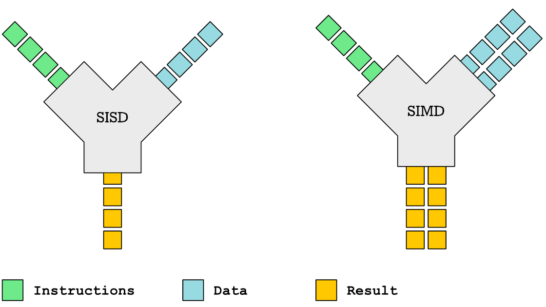
The instruction you see fed in here are things like add, multiple, subtract, shift and divide. The data is the numbers we are performing these operations on.
This story got a lot longer than planned, so I will give some bullets points with a short description of each main section:
- Operations of Simple RISC Microprocessor — Explain how a simple RISC processor execute instructions to contrast with how SIMD instructions are performed.
- How SIMD Instructions Work — Look at code examples with some known packed-SIMD instruction sets and try to understand how they work with some diagrams.
- From Packed SIMD to Vector Processing — How vector processing as found in old Cray computers as well as modern instruction set extensions such as ARM’s SVE2 and RISC-V’s V extension.
- Partitioning Tasks Across Multiple Cores — What if you want to make hundreds of SIMD enabled cores? How do you manage workloads across that many cores?
- Single Instruction Multiple Threads — SIMT — How modern graphics cards and AI accelerators from companies such as Nvidia solve the problem of distributing tasks across large number of cores with SIMD-like capabilities.
- Organizing and Managing Threads in Warps — Explanation of the thread concept in GPU programming and how it differs from normal CPU threads.
- Does GPU Hardware Need to Be This Complex? — A comparison and reflection on the difference in complexity in vector processing and SIMT based processing originating on graphics hardware.
Operations of Simple RISC Microprocessor
A microprocessor is made up of different functional units, drawn as gray boxes. Each gray box process data in some manner. When data is processed it has to be shipped to another functional unit over a data bus (blue arrow) or over an address bus (green arrows). You can think of the colored arrows as copper traces or wires sending electrical signals and the gray boxes as clusters of transistors that work together to accomplish a particular task.
To clarify this is just a way to get you to think about it. A microchip made out of silicon wafers does of course not have copper traces like you find on a printed circuit board.
The core of the CPU is the Arithmetic Logic Unit (ALU) which is like the calculator of the microprocessor. It reads numbers it adds subtracts or shifts from the registers. In a typical RISC processor you got 32 registers, which each can hold a number.
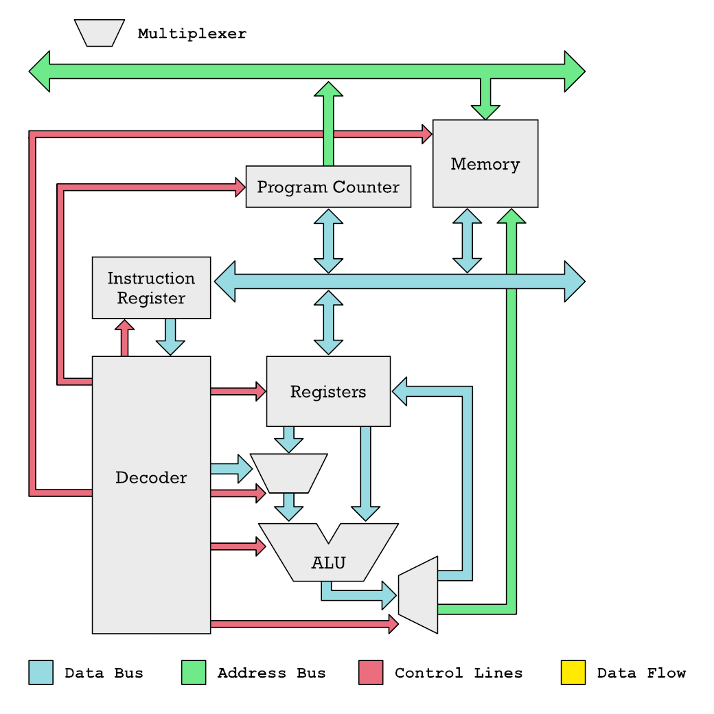
To decide exactly what arithmetic operation to perform the ALU has to be instructed what to do by control lines (red color), which are electrical signals which toggle on or off different functionality. The Decoder unit is in charge of toggling these control lines. The Decoder figures out what control lines to turn on or off by reading an instruction from the Instruction Register. We get instructions into the Instruction Register by reading them one by one from memory where you got your programs stored.
The diagram below shows how the Program Counter tells the Memory what address to read, and how the data at that address is then sent to the instruction register.
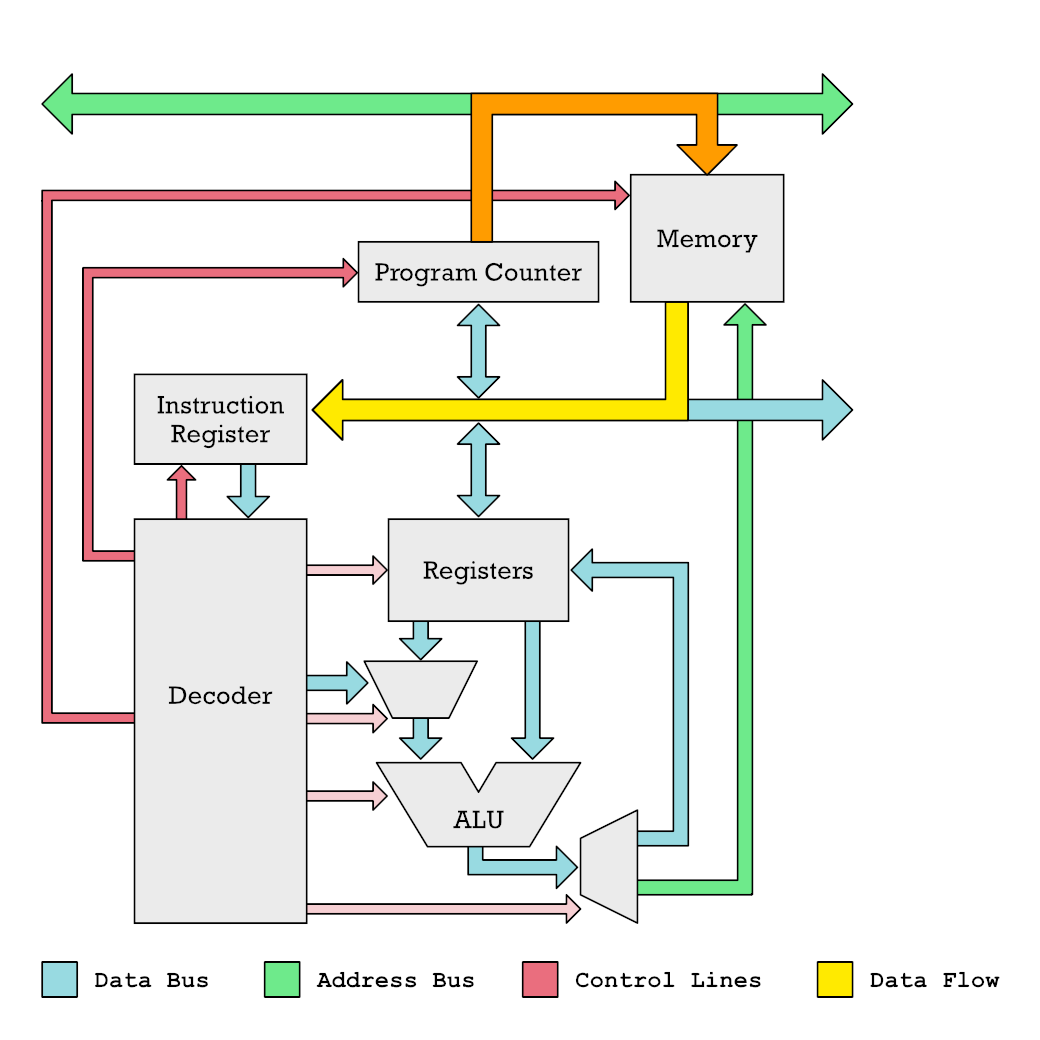
This gives you a little bit of context for how a CPU normally operates. It shuffles data around with the aim of feeding an ALU with data. Results are then send back to a register, next another instruction may store that into a memory location.
Here is a simple RISC-V assembly code program which shows something similar. Every instruction as you can see are very basic. LI (Load Immediate) loads a number into a register. That is all it does. ADD instructs the ALU to add two numbers together.
# RISC-V Assembly code for adding numbers 42 and 12

LI  x2, 42      # store 42 in register x2
LI  x3, 12      # store 12 in register x3
ADD x4, x2, x3  # add x2 and x3, result in x4
SW  x4, 90(x0)  # store result at memory location 90 + x0
Next step is to understand better how we can move from adding just single pairs of numbers to adding multiple pairs of numbers in a SIMD fashion.
How SIMD Instructions Work
In a simple processor we have registers and the ALU organized as shown in the diagram below. Some register r1 and r2 are used as inputs and the result is stored in another register r2. Of course any register could be used. Depending on the architecture they may be named x0, x1, ..., x31 or they could be r0, r1, ..., r15 as is the case on 32-bit ARM architecture.

To support SIMD instruction we add more ALUs to our CPU and segment registers into multiple elements. Thus we could take a 32-bit register and split it into two 16-bit elements which can be fed to a separate ALUs. Now we are suddenly able to double the number of arithmetic operations we are performing each clock cycle.
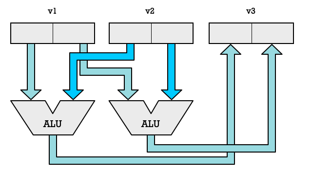
We don’t need to limit ourselves to two ALUs, we could add a lot more. If we have four ALUs we can process four number pairs in parallel. Each element pair combined with an ALU is called a SIMD lane. With two lanes we can process two pairs of numbers. With eight lanes we can process eight numbers in parallel.
How many number we can process in parallel is limited by the length in bits of our general purpose registers or vector registers. On some CPUs you perform SIMD operations on your regular general purpose registers. On others you use special registers for SIMD operations.
Let us use RISC-V as an example because it offers a fairly simple instruction-set. We are going to use the ADD16 and ADD8 instructions in the RISC-V P Extension.
The LW (Load Word) instruction will load a 32-bit value on a 32-bit RISC-V processor (RV32IP). We can treat this value as being two 16-bit values and add them up separately. That is what ADD16 does.
# RISC-V Assembly: Add two 16-bit values.

LW    x2, 12(x0)   # x2 ← memory[x0 + 12]
LW    x3, 16(x0)   # x3 ← memory[x0 + 16]
ADD16 x4, x2, x3
SW    x4, 20(x0)   # x4 → memory[x0 + 20]
As an alternative we could use ADD8 instead which would treat the 32-bit values we loaded from address 12 and address 16 as four 8-bit values.
# RISC-V Add four 8-bit values.

ADD8  x4, x2, x3
If we use Arm processor the logic will be quite similar even if the instructions will have slightly different syntax. Here is an example of using Arm’s Neo SIMD instructions with sixteen 8-bit values. Notice that Arm use the convention of adding suffixes to each vector register (r0, r1, ... r31) to indicate the size and number of elements. So a .16B suffix means sixteen elements and the B means byte sized elements.
; ARM Neon Add sixteen 8-bit values with (128-bit vector regs)

LDR v0, [x4]    ; v0 ← memory[x4]
LDR v1, [x6]    ; v1 ← memory[x6]

ADD v4.16B, v0.16B, v1.16B
STR v4, [x8]    ; v4 → memory[x8]
If we wanted to add 32-bit values, then those are referred to as single-word values or S for short.
; ARM Neon adding four 32-bit values
ADD v4.4S, v0.4S, v1.4S
Intel x86 SSE instructions are a bit more simple, as they originally just supported 32-bit element values. They added new registers named xmm0, xmm1, ... xmm7 which were all 128-bit. This gave each instruction the ability to process four 32-bit values.
; x86 SSE adding four 32-bit values

MOVAPS xmm0, [12]  ; xmm0 ← memory[12]
MOVAPS xmm1, [28]  ; xmm1 ← memory[28]
ADDPS  xmm0, xmm1
MOVAPS [44], xmm0  ; memory[44] ← xmm0
SIMD processing can happen in many different ways. What we have just seen in called packed-SIMD instructions. But vector-SIMD instructions also exist.
With packed-SIMD instruction we are also explicit about the the size of the elements we are operating on and the number of elements we are operating on. Notice how the Arm Neon packed-SIMD instructions require you to give a suffix like .16B or .4S to the registers. Those suffices state exactly how many elements we process and how wide each one is.
RISC-V P Extension is slightly more flexible here in that the number of elements is actually determined by whether the CPU is 32-bit or 64-bit. On a 32-bit RISC-V processor the ADD16 instruction use two 16-bit numbers per input register, while for a 64-bit processor it uses four 16-bit numbers per input register.
Bottom line is that all these packed-SIMD instruction sets are limited by the fact that they severely limit the ability to expand the size of elements and the number of elements which can be processed without adding more instructions. The code below encode two entirely different instructions. If you want to support another suffix, you need to add more instructions to the instruction-set.
; ARM Neon
ADD v4.16B, v0.16B, v1.16B
ADD v4.4S, v0.4S, v1.4S
This requirement is a major limitation on packed-SIMD instructions. What we want instead are higher level abstractions which allow hardware designers to add more processing capability without having to change the interface to our hardware each time.
From Packed SIMD to Vector Processing
We want to be able to add more SIMD lanes and have larger vector registers, but we cannot do that without adding new instructions when following the packed-SIMD approach.
One early solution to this problem which was used by Cray super computers back in the 70s and 80s was to define vector-SIMD instructions. With these instructions vector registers are thought of as typeless. The vector instructions don’t say anything about how many elements we have and their size.
This is the strategy used by RISC-V Vector extensions (RVV) and Arm Scalable Vector Extensions (SVE). With RVV se use an instruction called VSETVLI to configure the size of our elements and number of elements. We fill a register with how many elements we want to process each time we perform a SIMD operation such as VADD.VV (Vector Add with two Vector register arguments).
For instance this instruction tells the CPU to be configured to process 16-bit elements. x2 contains how many elements we want to process. However, our SIMD hardware may not have enough large enough registers to process that many 16-bit elements, which is why the instruction will return in x1 the actual number of elements we are able process each time we call a vector-SIMD instruction.
VSETVLI x1, x2, e16In practice we have to specify elements size when loading and storing because it influences the ordering of bits. Hence we issue a VLE16.V to load x1 number of 16-bit values. VLSE16.V is used to store x1 number of 16-bit values.
# RISC-V Vector processing (adding two vectors)

VSETVLI  x1, x2, e16 # Use x2 no. 16-bit elements
VLE16.V  v0, (x4)    # Load x1 no. elments into v0
VLE16.V  v1, (x5)    # Load x1 no. elments into v1
VADD.VV  v3, v0, v1  # v3 ← v0 + v1
VLSE16.V v3, (x6)    # v3 → memory[x6]
With vector-SIMD instructions we abstract away how many SIMD lanes we have from the instruction-set. The illustration below shows how vector processing works. Each register has 16 elements, but only two SIMD-lanes. That is not a problem because a vector processor will simply cycle through all the elements until done. In a packed-SIMD we would have processed two pairs of numbers in a clock cycle. With vector-SIMD we spend four CPU clock cycles to get through eight pairs of numbers.
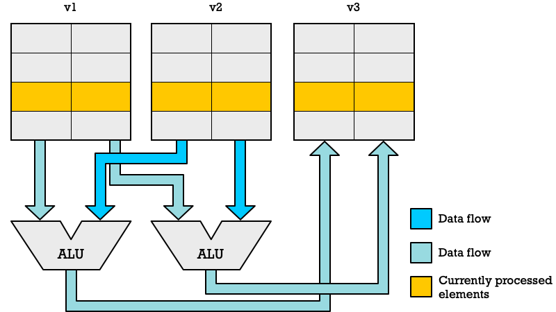
If we had had four SIMD lanes (four ALUs) we could have processed eight pairs of numbers in just two clock cycles. The beauty of this approach is that you can run the exact same code on different CPUs which different number of SIMD lanes.
Thus you could have a cheap microcontroller with just a single-lane or a complex high-end CPU for scientific computing with 64 SIMD-lanes. Both would be able to run the same code. The only difference would be that the high-end CPU would be able to finish faster.
Partitioning Tasks Across Multiple Cores
We are not actually done abstracting SIMD computations. We can go much further. To get maximum performance we want to be able to do as much work as possible in parallel, but we are not always going to need to do exactly the same operation on huge number of elements. That is why it makes sense to have multiple CPU cores. Also because there is a lot of non-vector code you might want to do in parallel with vector processing.
There are different ways of going about this. A modern CPU core is extremely large because it contains a lot of transistors to pull off lots of tricks which allows it to execute many instructions in parallel. This is what superscalar processors do. The diagram below may give you an idea. Notice that unlike or initial simple diagram this one has multiple instruction decoders at the bottom. Instead of a decoded instruction immediately toggling various control lines to control different units such as the ALU, we create micro-operations.
The CPU contains various clever stuff that figures out which of these micro-operations do operations which are independent of each other, so that operations can be done in parallel. Perhaps it figures out that there is a multiplication which does not depend on an addition instruction which got decoded. In that case the Multiplier and the ALU can work in parallel.
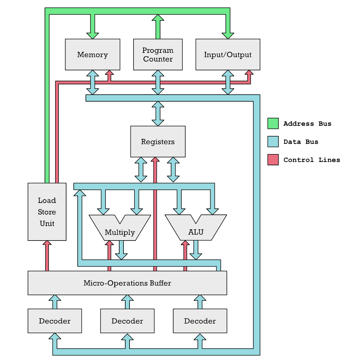
To get even fancier a superscalar CPU can execute instructions Out-of-Order (OoO), which means it figures out a way to reorder them to more easily run things in parallel. Later it has to order the results back again.
Okay, okay I know, you are wondering what the hell this has to do with SIMD instructions. To be fair it doesn’t directly have anything to do with SIMD. It is simply a detour to get you to understand why modern CPUs pack so many transistors. They do a lot of clever stuff which requires a lot of transistors.
On the other hand if your processor cores are supposed to mainly perform lots of SIMD instructions you don’t need all that fancy stuff. It is just dead weight. In fact if you throw out superscalar OoO capability, fancy branch predictors and all that good stuff you get radically smaller processor cores. In fact an In-Order SIMD oriented core can be made really small.
Say you have 20 billion transistors to play with. You could make perhaps 16–32 fat cores with that transistor budget. But if you make simple vector processing cores you could make a thousand vector processing cores!
So now you have a thousand cores which each have say 512-bit vector registers letting you process 32 16-bit values on each clock cycle (512/16 = 32).
Maybe you have a million elements you want to process. You need some higher level abstraction to divide up the work and push it out to each of your thousand vector processing cores. Together all these cores can process 32 000 elements (32*1000) each CPU cycle assuming memory is not a bottleneck.
What I have just described is essentially what Esperanto Technologies are doing with their RISC-V based AI accelerator card. They have made a System on a Chip (SoC) called ET-SOC-1 which has four fat superscalar general purpose cores called ET-Maxion. In addition they have 1088 tiny vector processor cores called ET-Minion. Now the later are also general-purpose CPUs but they lack all the fancy superscalar OoO stuff which makes them run regular programs fast. Instead they are optimized for vector processing (vector-SIMD instructions).
Let me recap what we have learned this far:
- We looked at regular dumb RISC processor with scalar operations.
- Then we thought: Hey let’s pretend a register is an array of numbers and let’s do computations on each of these numbers in parallel by adding more ALUs and multipliers.
- First simple approach to utilizing these multiple ALUs and vector registers is by defining packed-SIMD instructions.
- Packed-SIMD doesn’t scale over time. Need new instructions every time hardware designers wants to add more SIMD lanes. vector-SIMD to the rescue.
- Single cores with vector-SIMD is not enough. We need more cores. Now we got a new problem: How do we organize and split up the workloads?
Before Esperanto Technologies, graphics cards makers such as Nvidia have been solving this exact same problem. A graphics card isn’t just a single core working on really long vector registers. Just like ET-SOC-1 they contain huge number of small cores optimized to run SIMD instructions.
But now things get a lot more complicated.
Single Instruction Multiple Threads — SIMT
With graphics hardware things get a lot more complicated. When I started writing this story my intention was to explain graphics hardware as SIMD processing with higher level stuff on top.
Yet, that is not a fair characterization. What graphics cards makers would call SIMT — Single Instruction Multiple Threads — is significantly different from SIMD that it deserves its own abbreviation.
Instead of talking about SIMD lanes graphics guys talk about threads. At first I thought this was abuse of well known terminology. Normally a thread encapsulates a thread of execution. It requires storing a program counter which says where in program a particular thread is.
You got a scheduler which can resume a thread. It will then pop from storage the program counter for that thread to resume execution at its last location in the program when the thread to paused.
Threads are practical in normal software because you can have code reading and writing to disk or network, which gets stuck waiting for a response. With threads, you can halt a thread which is waiting for data and resume another thread to do useful stuff.
This doesn’t sound much like SIMD lanes right? So how has this terminology snuck in when discussing parallel processing in GPUs? It is because SIMD lanes on a GPU core is in fact a lot more like a thread.
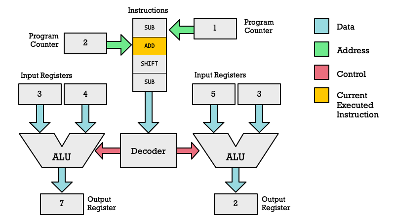
It is not just that a lane as its own computational unit such as an ALU, but they also have their own program counter (PC) and their own load store unit (LSU). What? So you each SIMD lane can run instructions completely independent like a normal CPU core?
Not exactly. On an Nvidia GPU you basically have 32 SIMD lanes. One instruction can be performed on 32 pairs of numbers at the same time. Interestingly conditional instructions are still allowed. Say a condition is true for 12 threads (lanes) and false for 20 threads. That means different code needs to be run for both of these groups of threads. Each one get their program counters updated, but we only run the threads with the same program counters at the same time.
Thus first 12 threads may run an ADD instruction. Perhaps they run yet another one, a SHIFT (multiply by factors of two) instruction. Every time the program counter (PC) gets updated for each of the 12 threads.
At some point you may reach an instruction which reads data from memory. That turns things on their head. With packed-SIMD and vector-SIMD we are responsible for filling in the vector registers from memory before the SIMD engines get to do their job. With SIMT it is different: Each “lane” gets to pull data from memory itself. Every lane executes a load from memory instruction, but registers may point to different memory addresses.
Memory reads are often slow, so at this point the 12 threads may be paused. At this point we run the 20 other treads which have the same program counter position. Perhaps they execute as SUB (subtract) instruction. Threads not run are masked.
Masking is something which is possible with packed-SIMD and vector-SIMD (vector processing), but which was not supported on early SIMD instruction-sets. It basically allows you to disable certain elements (lanes) when doing a particular computation.
Let us summarize the key points:
- Every thread in a GPU core has its own program counter, pointing to different locations in their shared program (kernel).
- Only one instruction can be executed at at time. However, this instruction is repeated across all threads with the same program counter.
- Each instruction is performed on a maximum of 32 threads in parallel.
Parallel Memory Access with LSUs
Every thread (SIMD lane) gets its own LSU when running. An LSU which computes memory addresses. It means every thread can perform read and write instructions to memory.
Obviously multiple threads running in parallel performing a load operation cannot read from multiple memory locations at the same time, since memory is a shared resource. Instead both CPUs and GPUs read memory in chunks. The chunks tend to be 64 or 32 bytes. Thus LSU addresses are put into groups. Many LSU memory addresses will fall within the same 32 byte chunk. We read one chunk at a time. That means each clock cycle only some of the active threads get the data they requested.
I have tried to illustrate this in the diagram below. To simplify I have removed the instruction stream, program counter and instruction decoder from this diagram to focus on the interaction between memory and registers. Basically this diagram shows two lanes which can execute two GPU threads in parallel.
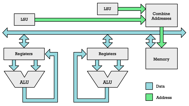
Since getting data for every SIMD lane can take multiple cycles, graphics card makers try to optimize the system by scheduling new tasks. That brings us to the next concept: warps and warp schedulers.
Organizing and Managing Threads in Warps
With Nvidia speak, we call a GPU core for a Symmetric Multiprocessor (SM). Each of these GPU cores can execute one instruction on 32 threads at the same time. You can think of each GPU core as having SIMD engines with 32 lanes.
This characterization is a simplification because each core can have from 1–4 SIMD engines, each performing one operation on 32 threads in parallel.
We just talked about how memory access can take multiple cycles. Thus to utilize the GPU cores more effectively we switch between threads. This is just like regular multithreading. If one thread is stuck waiting for input data on a regular CPU, you switch to another thread.
The same thing happens on GPUs except each thread cannot run instruction independently of each other they are bundled into what is called a warp (Apparently in weaving terminology a warp is a bundle of threads).
The GPU cores (SMs) can store the state of many warps and schedule a new warp each time another one is stalled. This allows more efficient utilization of the processing capability in the SIMD engines of the GPU cores. Instead of them sitting idle while waiting for input data another warp can be woken up and continue processing.
These switches between warps is very quick and not like switching between threads in a CPU. My understanding is that you can rapidly switch between multiple warps and only do one instruction per warp without incurring an overhead doing so.
The diagram below is trying to illustrate how this scheduling works in a GPU core with two warp schedulers. You got four different warps with their own sequence of instructions to be processed. Notice how the instructions for each warp is executed in sequence, but other warps can get interleaved.
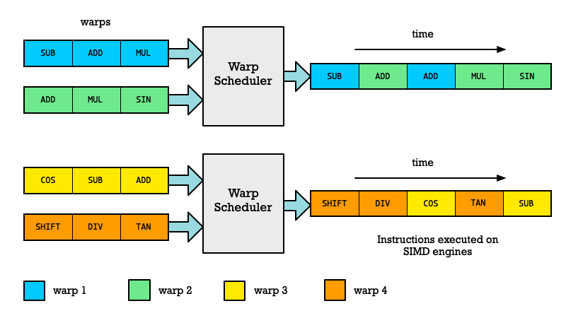
If you are more interested in the details, you could read the whitepaper for the Nvidia Fermin microarchitecture.
Organizing Work Into Thread Blocks
We have looked at the lowest levels of how instructions are executed in a SIMT architecture, but not how chop up say one million elements and process them in chunks. To explain that we will look at some matrix and vector math related code.
Digression About Linear Algebra and SIMD Code Examples
The math around matrices and vectors is called Linear Algebra. It contains info about matrix multiplication, inversing matrices and many other things. Since this is so important in all science and engineering we have had a Fortran library called BLAS and LAPACK for many decades with a rich collection of functions for doing Linear Algebra. This is sort of the gold standard.
Because Linear Algebra involved matrices and vectors, it is a popular target for any system doing SIMD based processing. Thus whether looking at RISC-V vector extension examples or Nvidia CUDA or OpenCL example code you are going to see mentions of cryptically named functions such as SAXPY and SGEMM.
These functions are popular in all SIMD related code examples, so we will use them here to explain how threads are organized into thread blocks in SIMT based code. SAXPY calculates:
Y = αX + Y # saxpyWhere X and Y are matrices (or vectors) and a is a scalar. Every BLAS function is about doing these sort of simple operations. SGEMM for instances does the following operation:
C = aA⋅B + βC # sgemmIt is common in Linear Algebra to use capital letters for matrices and lowercase letters for scalars. In my programming examples I will use xs and ys to denote arrays of elements. Thus x would be an element in xs and y an element in ys.
Implementing SAXPY
Normally you would implement SAXPY like this to run on a CPU.
// Single-Precision α ⋅ X Plus Y,
void
saxpy(int n, float a, float *xs, float *ys) {
    for (int i=0; i<n; i++)
        ys[i] = a * xs[i] + ys[i];
}
To make it run on a GPU we define a function which will normally be referred to as a kernels. A kernel usually denotes a snippet of code applied to a large number of elements. This syntax is based on CUDA (Nvidia).
Notice that the for-loop is gone. Instead the code is made to execute on one SIMD lane in a SIMT processor. This code will run on a GPU rather than on the CPU, so the kernel code will be compiled by the graphics drivers and pushed out to the GPU.
_global_void
gpu_saxpy(int n, float a, float *xs, float *ys) {
    int i = blockIdx.x * blockDim.x + threadIdx.x;
    if (i < n)
        y[i] = a*xs[i] + ys[i];
}
Read more: CUDA example code.
The graphics card doesn’t do that itself, so you need to run some code on the CPU which sets everything up. We got two arrays xs and ys of n elements which we want to process. To do the job in parallel we want to split up this task into multiple chunks. In OpenGL they aptly name it a work group. Nvidia calls it a thread block. Each GPU core can process one thread block.
// Invoke parallel SAXPY kernel (256 threads per block)

int blocksize = 256
int nblocks = (n + blocksize-1) / blocksize;
saxpy_parallel<<<nblocks, blocksize>>>(n, 2.0, xs, ys);
Because we are often working with matrix data a system has been made which makes it easy to figure out which row and column of a matrix a thread is assigned to work on. This is called the thread index. The GPU machinery that schedules threads to warps doesn’t care about the thread index but relate to the thread ID. The thread ID is what uniquely identifies a particular thread.
If I work on a matrix and want to know in my kernel code what row and column I am processing then I can ask what the threadId.x and threadIdx.y values are. These are global variables that map to registers in each GPU core (SM). If I worked with a cube of data I might be interested in threadIdx.z as well.
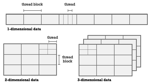
To utilize more GPU cores we cluster our threads into thread blocks. The hardware is setup so that each GPU core can process a thread block in parallel.
Now here is an important point to observe: A GPU core isn’t going to process every single thread at the same time. Remember it can only process 1–4 warps at the same time and each warp is 32 threads. Hence a maximum of 128 (4 × 32) threads can be processed at the same time in a GPU core.
Why Assign More Threads to a GPU Core Than it Can Process in Parallel?
If you cannot process all threads, then why not assign fewer threads to each core and spread them over more cores?
Now you got to remember what we said about warps stalling because of waiting for memory. All sorts of stuff can happen which means the current instruction in a warp cannot be executed.
To be able to utilize hardware resources effectively, we want to have other warps ready to take their place. Thus even if you core could only do 64 threads in parallel, you should still assign more threads to keep the SIMD engine busy.
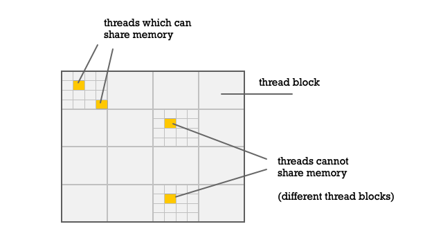
The second important point is that threads within a block can share memory. Remember each GPU core has its own local memory. That means the load/store instructions executed on the same GPU core is able to access the same memory.
Thus if threads need to shared results with each other they need to be on the same thread block.
Block Sizes Will Not Always Match Your Array
Say you want to process two arrays which have 80 elements. If you use one 64 element block you cannot process the whole array. If you use two 64 element blocks you get 128 elements which is too many. This is why the saxpy implementation has these lines:
if (i < n)
        y[i] = a*xs[i] + ys[i];
Remember the kernel gets called based on the thread block configuration you have setup, not based on the number of elements your array actually had.
Thus we must make sure we don’t make a calculation for every thread index. Some will be out of bounds.
How Are Threads Mapped To Warps?
When working with 1D data your thread ID and your threadIdx.x will be the same. Threads with ID 0, 1, ... 31 will form one warp while threads with ID 32, 33, ... 63 will form the next warp.
That means when we execute the if-statement if (i < n), it will happen within a warp where the condition will be true for some of the threads and false for others.
The threads for which the condition is untrue will simply be masked (program counter not updated) while instructions for the following code is run:
y[i] = a*xs[i] + ys[i];Using masks is a common strategy in all vector processing today. Yo will find this in both vector-SIMD and packed-SIMD instructions. RVV, SVE and AVX all use masks. It is to deal with the common problem that the number chunks of elements processed by a SIMD engine will seldom neatly divide up the whole array of data your are processing. You will usually get a tail-end.
Early packed-SIMD instructions did not support masks and thus one had to handle the tail end of a vector with regular scalar instructions, making the processing of the tail end quite slow.
Does GPU Hardware Need to Be This Complex?
All hardware that aims to schedule numerous workloads to different cores will incur some complexity. However, I think it is a still a fair question to ask.
The SIMT hardware concept makes sense from a historical perspective. The graphics pipeline usually fed vertices from 3D models to the a kernel we call a vertex shader. Later the pipeline would generate fragments (pixels with depth) for surfaces formed between vertices. Each of these fragments would run a fragment shader (kernel).
Each one would want to do a fair amount of complex things. You would want to do a matrix multiplication of the vertex coordinates to do projection transformations, move the camera in the scene and many other things. For fragments you would want want to lookup texture data.
That is a lot of complex stuff for every “SIMD-lane” and thus the traditional SIMD thinking had to be heavily augmented to the point where we got SIMT which started to look increasingly like little CPU cores themselves. Perhaps why Nvidia calls them cores even if they are sort of like amped up SIMD lanes.
For many machine learning (ML) and many scientific tasks, this approach is not necessarily the most logical way of thinking about data processing. Even back in the 1980s a compiler could take code looking like this:
void
saxpy(int n, float a, float *xs, float *ys) {
    for (int i=0; i<n; i++)
        ys[i] = a * xs[i] + ys[i];
}
And turn it into vectorized assembly code. We can look at the modern RISC-V vector extension variant. Sure it is assembly so it is more book keeping and harder to follow. Yet in conceptual terms this is way simpler than what GPU cards are doing.
All this code does is figure out how many elements our vector processing hardware can process, then load that number of elements into vector registers. Then we call the vfmacc.vf assembly code instruction which does the whole calculation.
Every iteration we take another chunk and load it up for processing.
saxpy:
    # t0 ← min(a0, (VLEN × 8) / 32)
    vsetvli t0, a0, e32, m8, ta, ma

    vle32.v v0, (a1)    # v0 ← mem[a1:a1+t0]

    sub a0, a0, t0      # calc xs elements left to read
    slli t0, t0, 2      # t0 << 2 (each element is 4 bytes)
    add a1, a1, t0      # point a1 to next xs batch to read

    vle32.v v8, (a2)    # v8 ← mem[a2:a2+t0]
    vfmacc.vf v8, fa0, v0  # v8 ← fa0 × v0 + v8

    vse32.v v8, (a2)    # store batch of results at a2
    add a2, a2, t0      # point a2 to next ys batch to read
    bnez a0, saxpy      # goto saxpy if a0 ≠ 0
    ret
This is perhaps also why we are starting to see various vendors challenging the hegemony of the big beefy graphics cards for scientific computing and machine learning. You don’t need as complex hardware to process a lot of this kind of data.
Take Machine Learning and Deep Neural Networks as an example. Most of what you are doing is multiplying and adding large matrices. That problem domain can be expressed with a much simpler interface than what you get from something like CUDA.
So why have 3D graphics card and their descendants dominated this market so long? I am no expert in this area so this will be a bit of speculation: Companies like Nvidia have built up competency and volume in making beefy graphics card. It makes sense to tweak their core technology to expand into new markets.
CUDA was built upon the peculiarities of how graphics hardware works. For Nvidia and others it doesn’t make a lot of sense to abandoned a platform which already dominates the market.
An analogy might be the x86 CPU market. We all know that the x86 instruction-set is not optimal anymore. It is a totally outdated instruction-set (ISA). Still it is an ISA which dominates the current market. Rather than create a clean design it made more sense for Intel and AMD to tweak the existing design by adding new powerful instructions, throw in a RISC-like engine inside and add all sorts of other expensive tricks to keep the competition at bay.
When superior RISC chips in the 90s challenged Intel, they got beaten because with superior volume and profits Intel was able to throw money at their problems and outspend the RISC guys.
I suspect a similar strategy is what gave us graphics cards as AI accelerators. They may not be an idea platform but companies like Nvidia have kept them in the game by throwing in lots of new special features such as Tensor cores to keep these card competitive.
But eventually you may reach an inflection point as we see with x86 vs ARM today. Eventually legacy catches up with you and the benefits of a cleaner design wins the day.
Summary and Final Remarks
If you read this to the end: Congratulations. This story took on a life of its own. I very much wished I could have written a tighter cleaner version of this. But as Blaise Pascal said: “Sorry about the long letter, I did not have time to write a shorter one.”
I decided to push out this version rather than spend time writing a shorter version. Anyway I want to try to summarize what this was about.
Modern high performance computing is all about parallelism of some kind. Either we find instruction level parallelism using superscalar CPU cores, or we do task parallelism by creating multiple cores. Each core can run a hardware thread, performing a different task.
Finally we can exploit data parallelism which has been the focus of this article. That is to deal with the cases where the same operation can be applied to multiple elements at the same time. It is something that arises in scientific computing, linear algebra, computer graphics, machine learning and many other fields.
I tried to build up your understanding by starting with the simplest way of doing it:
- Packed SIMD instructions — Specific instructions which say: “multiply register v0 with v1, where both have eight 32-bit elements.”
- Vector SIMD instructions — We move up in abstraction and hide how many SIMD lanes we got. Hardware architects can beef up CPUs without changing instruction-set.
- Single Instruction Multiple Threads (SIMT) — Means each SIMD lane is now executing a whole bunch of instructions. They can even read memory, keep track of where they are in the program (program counter register) etc.
With GPUs we got a whole new level of abstraction. You will never look at the assembly code generated. You send high level code to a driver which compiles it. The capabilities of the hardware has been substantially abstracted.
However, the abstraction may not work perfectly for the simple reason that GPU cores are not general purpose processors. Regular C code could be compiled to vectorized code. You cannot do that with GPU code. You have to be pretty explicit that you are actually targeting a GPU by specifying things such as number and size of thread blocks.
Related Stories
Stories I have written about hardware which may be of interest.
- RISC-V Vector Instructions vs ARM and x86 SIMD — Focused on comparing packed-SIMD and vector-SIMD instructions and why they exist.
- ARMv9: What is the Big Deal? — Goes into more details about the SVE2 vector-SIMD instruction set added to the ARMv9 architecture.
- The Genius of RISC-V Microprocessors — Nothing about SIMD but about instruction compression and macro-operation fusion in RISC-V cores.
- How Does a Modern Microprocessor Work — Meant as a beginners introduction to how a microprocessor works. We look at a simplified RISC processor. It operates on decimal numbers rather than binary numbers to simplify explanation.
Resources
- CUDA C++ Programming Guide — Great Nvidia guide detailing threads and blocks with good matrix multiplication example.
- CUDA Binary Utilities — Explanation of GPU assembly code by looking at assemblers/disassemblers for CUDA.
- More compute shaders — Explanation of how shader assembly instructions work.
- ARB assembly language — A low level shading language a bit similar to assembly. Old OpenGL stuff.


